
")
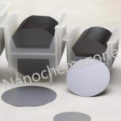
Single Crystal Silicon Wafer Intrinsic (2 Inch)
$0.00
In StockSingle Crystal Silicon Wafer Intrinsic (2 Inch)
Product Name: Single Crystal Silicon Wafer Intrinsic (2 Inch)
| Product Name | Single Crystal Silicon Wafer Intrinsic (2 Inch) |
| Cat No. | NCZ-NSC328/20 |
| Size | 50.8+/- 0.2mm, |
| Thickness | 430+/-10um |
| Undoped | Intrinsic |
| Resistivity | 2000~4000Ω.cm |
| Orientation | <100>+/-0.5° |
| Polishing | One Side Polished |
Provided in a single wafer case
Description:
Single Crystal Silicon Wafer Intrinsic is the most widely used semiconductor material as a substrate material due to its excellent machinability, mechanical stability, and the potential to combine sensing elements and electronics on the same substrate.
Circular wafers made of silicon are used as a substrate in most MEMS sensors. The crystal orientation should be known before manufacturing since silicon has orientation-dependent properties such as piezoresistivity coefficients and etching rates. The common orientation is (100) where the numbers represent Miller indices.
As an example, (100) wafer that has a primary flat side as an indication of < 110 > direction. When a piezoresistive element is placed on a (100) wafer, the orientation should be parallel to < 110 > direction if the piezoresistivity coefficients in that direction are intended to be utilized.
Description
Note: For pricing & ordering information, please contact us at sales@nanochemazone.com
Please contact us for quotes on Larger Quantities & Customization. E-mail: contact@nanochemazone.com
Customization:
If you are planning to order large quantities for your industrial and academic needs, please note that customization of parameters (such as size, length, purity, functionalities, etc.) are available upon request.
Related products
-

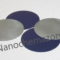
Single Crystal silicon-silicon dioxide Wafer
Product Name: Single Crystal silicon-silicon dioxide Wafer
Product Name Single Crystal silicon-silicon dioxide Wafer P-type (4 inches) Cat No. NCZ-NSC318/20 Día 100 mm (4 inches) Orientation <100> Wafer thickness 500 micrometer Resistivity <0.01 Polished Front Side Polished Thickness 300 nm (dry) Purity 99.9% Formula Si/SiO2 Single Crystal silicon-silicon dioxide Wafer P-type Description :
Provided in a single wafer case
Silicon oxide wafer SIO2 thin-film among semiconductor technology, SiO2 thin film layers are mainly used as dielectric material and more recently, they are integrated with MEMS (Micro Electro Mechanical Systems) devices. The simplest way to produce silicon oxide layers on silicon wafers is to oxidize silicon with oxygen.
Single Crystal silicon-silicon dioxide Wafer RELATED INFORMATION
Storage Conditions:
Airtight sealed, avoid light and keep dry at room temperature.
Please email us for the customization.
Email: contact@nanochemazone.com
Note: We supply different size ranges of nano and micron size powder as per the client’s requirements and also accept customization in various parameters.
$0.00 -
 2")
Single Crystal Silicon Wafer Diameter Intrinsic (4-inch)
Product Name: Single Crystal Silicon Wafer Diameter Intrinsic (4-inch)
Product Name Single Crystal Silicon Wafer Cat No. NCZ-NSC327/20 Diameter 4 inches Doping undoped Thickness 400~415+/-10um Resistivity 4000 5000 ohms.cm Undoped Orientation <100>+/-0.5 Polishing one side polished Application Research Material Thickness 525 Micron Resistivity 1-10 ohm-cm Polished Single side polished Provided in Single wafer case.
Description:
Single Crystal Silicon Wafer thickness Is determined by the mechanical strength of the material used the wafer must be thick enough to support its own weight without cracking during handling. Wafers are grown from crystal having a regular crystal structure, with silicon having a diamond cubic structure. Orientation is defined by the Miller index with (100) or (111) faces being the most common for silicon. Ion implantation depends on the wafer’s crystal orientation since each direction offers distinct paths the transport.
Note: SSP = Single Side Polished, DSP = Double Side Polished, E = Etched, C = AsCut, Material – CZ unless noted, L = Lapped, Und = Undoped (Intrinsic)
$0.00 -
 3")
Single Crystal Silicon Wafer N-type (4-inch)
Product Name: Single Crystal Silicon Wafer N-type (4-inch)
Product Name Single Crystal Silicon Wafer N-type (4-inch) Cat No. NCZ-NSC331/20 Día 4 inches Type N Diameter (mm) 4” (100.8mm) Type N-Type Doping Phosphorous Crystal Orientation <100> Surface: Single Side Polished Thickness 250-500μm Resistivity 1-10ohm-cm Crystal method CZ RRG (%) ≤12 Oxygen Contents (ppm) 12.5-16.5 Carbon Contents (ppm) ≤1 Description:
Wafer resizing is sometimes referred to as wafer coring, re-sizing, cut down, cut-down, downsizing, down-sizing, size reducing or size reduction. We can accept orders ranging from a single wafer to hundreds of wafers per month. Our process is efficient, innovative, and ESD friendly. Our proprietary process causes less stress to the silicon wafer than other resizing methods. We also round wafer edges to eliminate edge chipping.
We frequently work with 2” (50 mm), 3” (75 mm), 100 mm (4”), 125 mm (5”), 150 mm (6”), 200 mm (8”), and 300 mm wafers; however, we are also capable of producing custom non-standard sizes.
Please email us for the customization.
Email: contact@nanochemazone.com
Please contact us for customization and price inquiry
Note: We supply different size ranges of Nano and micron as per the client’s requirements and also accept customization in the various parameters.
$0.00 -

Single Crystal Silicon Wafer P-type,
Product Name Single Crystal Silicon Wafer P-type Cat No. NCZ-NSC332/20 Día 3 inch
Diameter 76.2mm ± 0.3mm (3 inches) Type P Orientation <100> Thickness 400±10um Resistivity
1-10 ohm-cm
Polished
Single side polished
Provided in a single wafer case
Description:
Nanochemazone® Supplies provides both standard and customized high-quality single crystals, wafers and substrates for a wide range of applications such as LED, ferroelectric, piezoelectric, electro-optical, photonics, high power electronics, and high-frequency power devices, just to name a few. Customized crystal growth, precision machining, and coating services are available. Please contact us today to discuss your project requirements.
Related Information
Please email us for the customization.
Email: contact@nanochemazone.com
Please contact us for customization and price inquiry
Note: We supply different size ranges of Nano and micron as per the client’s requirements and also accept customization in the various parameters.
Note: For pricing & ordering information, please contact us at sales@nanochemazone.com
Please contact us for quotes on Larger Quantities & Customization. E-mail: contact@nanochemazone.com
Customization:
If you are planning to order large quantities for your industrial and academic needs, please note that customization of parameters (such as size, length, purity, functionalities, etc.) are available upon request.
$0.00 -
 5")
Single Crystal silicon-silicon dioxide Wafer N-type (4 inch)
Product Name Single Crystal Silicon Wafer P-Type (4 Inch) Cat No. NZC-NSC333/20 MF Si/SiO2 Día 100mm ± 0.5mm (4 inch) Type/Dopant P Orientation <100> Wafer thickness 525±25um Resistivity 1-10 ohm-cm Polished Single side polished TTV < 10um SiO2 Oxide Thickness 300 nm (dry) Provided in single wafer box
Crystal silicon-silicon dioxide Wafer N-type (4 inches) Description
Single crystal silicon is the most widely used semiconductor material as a substrate material due to its excellent machinability, mechanical stability, and the potential to combine sensing elements and electronics on the same substrate. Circular wafers made of silicon are used as the substrate in most MEMS sensors. The crystal orientation should be known before manufacturing since silicon has orientation-dependent properties such as piezoresistivity coefficients and etching rates. The common orientation is (100) where the numbers represent Miller indices. As an example, (100) wafer that has a primary flat side as an indication of < 110 > direction. When a piezoresistive element is placed on a (100) wafer, the orientation should be parallel to < 110 > direction if the piezoresistivity coefficients in that direction are intended to be utilized.
Note: For pricing & ordering information, please contact us at sales@nanochemazone.com
Please contact us for quotes on Larger Quantities & Customization. E-mail: contact@nanochemazone.comCustomization: If you are planning to order large quantities for your industrial and academic needs, please note that customization of parameters (such as size, length, purity, functionalities, etc.) are available upon request.
Crystal Silicon dioxide Wafer N-type (4 inches) RELATED INFORMATION
Storage Conditions:
Airtight sealed, avoid light, and keep dry at room temperature.
Please contact us for customization and price inquiry
Email: contact@nanochemazone.com
Note: We supply different size ranges of Nano and micron as per the client’s requirements and also accept customization in various parameters.
$0.00 -

Single Crystal Silicon Dioxide Wafer P-Type
Product Name: Single Crystal Silicon Dioxide Wafer P-Type
Product Name Single Crystal Silicon Dioxide Wafer P-Type Cat. No. NCZ-NSC 319/20 Diameter 100 mm +-0.2 mm (4″)
Oxide Thickness 300 ±20 nm (dry) Color Violet Thickness 500 ± 20 micron Resistivity
1-10 ohm-cm
Type/Dopant P Orientation <100> Single Crystal Silicon Dioxide Wafer P-Type (4 inches) Description
Single Crystal Silicon Dioxide Wafer P-Type Nanochemazone® produces Silicon Oxide Wafer with the highest possible density. Our standard wafer size is nominally 25.4 mm (1 inch) to 300 mm (11.8 inches). Materials are produced using crystallization, solid-state, and other ultra-high purification processes such as sublimation.
This process forms a cylindrical ingot which is then sliced and polished to form wafers. Nanochemazone® High Purity (99.999%) Silicon Oxide Wafers- Polished & Unpolished specializes in producing custom compositions for commercial and research applications and new proprietary technologies.
Nanochemazone® also casts any of the rare earth metals and most other advanced materials into rod, bar or plate form, as well as other machined shapes and through other processes such as nanoparticles and in the form of solutions and organometallics. We also produce Silicon as rod, pellets, powder, pieces, disc, ingot, wire, and in compound forms, such as oxide. Other shapes are available by request.
Single Crystal Silicon Dioxide Wafer P-Type (4 inches) RELATED INFORMATION
Storage Conditions:
Airtight sealed, avoid light, and keep dry at room temperature.
Please email us for the customization.
Email: contact@nanochemazone.com
Note: We supply different size ranges of nano and micron size powder as per the client’s requirements and also accept customization in various parameters.
$0.00
