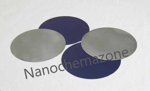
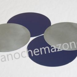
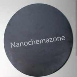
Single crystal silicon wafer Intrinsic (2-inch)
$0.00
In StockSingle crystal silicon wafer Intrinsic (2-inch)
Product Name: Single crystal silicon wafer Intrinsic (2-inch)
| Product Name | Single crystal silicon wafer Intrinsic (2-inch) |
| Cat No. | NCZ-NSC329/20 |
| Diameter | 2 inch |
| Doping | Intrinsic |
| Resistivity | (>1000ohm/sq.) |
| Thickness | 400µm |
| Orientation | 100 |
| Polished | Single side polished |
Provided in a Single wafer case:
Description:
Single crystal silicon wafer Intrinsic (2-inch) is the most widely used semiconductor material as a substrate material due to its excellent machinability, mechanical stability, and the potential to combine sensing elements and electronics on the same substrate. Circular wafers made of silicon are used as a substrate in most MEMS sensors.
The crystal orientation should be known before manufacturing since silicon has orientation-dependent properties such as piezoresistivity coefficients and etching rates. The common orientation is (100) where the numbers represent Miller indices.
As an example, (100) wafer that has a primary flat side as an indication of < 110 > direction. When a piezoresistive element is placed on a (100) wafer, the orientation should be parallel to < 110 > direction if the piezoresistivity coefficients in that direction are intended to be utilized.
Please email us for the customization.
Email: contact@nanochemazone.com
Please contact us for customization and price inquiry
Note: We supply different size ranges of Nano and micron as per the client’s requirements and also accept customization in the various parameters.
Description
Note: For pricing & ordering information, please contact us at sales@nanochemazone.com
Please contact us for quotes on Larger Quantities & Customization. E-mail: contact@nanochemazone.com
Customization:
If you are planning to order large quantities for your industrial and academic needs, please note that customization of parameters (such as size, length, purity, functionalities, etc.) are available upon request.

